Designing PCB layouts is both an art and a science, the design rules vary from design to design.
This section will explain some common practice and guidelines you can use for most designs.
1.
Always place your components before you start routing. When you place load your component footprints into PCBnew in KiCAD, they load in as a “rat’s nest”.
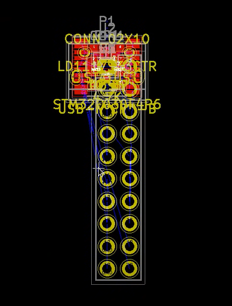
An example of the organized rat’s nest:
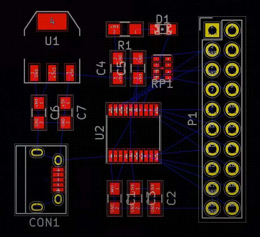
Here are some tips for component placement you should keep in mind. Place high pin count integrated circuits (IC’s) in central areas,
this will make routing to these IC’s easier. Try to minimize net crossing, nets are shown in KiCAD by the white lines connecting component pads.
Minimizing crossing nets will make routing easier and more direct. It will be impossible to completely stop nets from crossing in more complicated design,
try and minimize it the best you can. The figure below shows nets before they are routed.
When placing SMD components on the top and bottom layer of the PCB, keep in mind you could accidentally desolder components on the opposite side of the PCB.
This could happen if the component you are solder will require a lot of heat to solder on. Situation when components could require more heat to solder is
when they are connected to big power or ground planes. To avoid accidentally desoldering components try to place all components on one side if possible.
2.
When you start routing route power and ground traces first. Power and ground trace need to be bigger traces because they carry higher current.
To ensure there is enough space in your design for the larger traces they need to be routed first. To determine the size of trace required use a trace width calculator
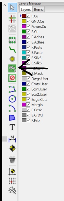
When routing power and ground planes that carry high current remember to use planes for this. To make planes in KiCAD click on the “Add Fill Zone” on the
right side tool bar.
3.
When routing remember to keep trace length short and as direct as possible. The length of the traces will matter if you are routing and high speed or analog
signals. Why and how the length of traces effects these signal goes beyond the scope of this tutorial, if you want to learn more about this read this.
Keeping traces as direct as possible is important because it keeps design neat which will make future routing easier. It also makes your design easier to
follow which will help if you need to troubleshoot your design later.
4.
While you are routing remember to use the Design rule check (DRC) button (the ladybug button on the top tool bar) often. This will help catch mistakes early,
catching mistakes early makes them easier to fix.
5. When you are placing IC’s that need decoupling capacitors remember to place them close to the pins that need them. An easy way to remember this is to
have the your KiCAD schematic open in another tab, when you click on components in the schematic they will highlight in the layout tab. If you are placing
your microcontroller and you need to place the decoupling caps near just click on the decoupling caps on your schematic and they will highlight in the layout tab.
This is a good practice to start because if decoupling caps are far away from the IC’s that need them, the IC’s might not function as intended. If you do not know
what a decoupling capacitor is see this article.
If you want to read more about PCB design guidelines read theses articles: